Design Idea

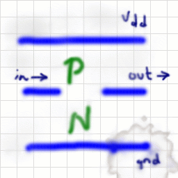
A simple signal flow diagram showing the connections to the inverter. All signals are horizontal and on the same metal layer.


A simple signal flow diagram showing the connections to the inverter. All signals are horizontal and on the same metal layer.


Cadence is a trademark of Cadence Design Systems, Inc., 555 River Oaks Parkway, San Jose, CA 95134.
Please read this DISCLAIMER