


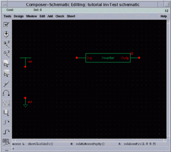
Note : You do not have to place the components exactly the same way as seen in the example images. As long as you connect them correctly, you can always move a component to some other location in the same schematic.
1. Pick up and place the rest of the components required for the simulation.
The remaining components are in the "NCSU_Analog_Parts" library. Change your library from "tutorial" to "NCSU_Analog_Parts". Refer to the previous example (step 3 :"Changing the library in the Component Browser window") to see how you can change the source library.
Open the folder "Supply_Nets", select "vdd" and "gnd" and place them anywhere in the schematic window. Your original circuit schematic already does have these supply nets attached to its appropriate nodes, but now you have to define the voltages in the new schematic window.
Go up one folder to the main content folder. Open the folder "Voltage Sources", select "vdc" and "vpulse" and place them in the schematic window.

Go up one folder to the main content folder. Open the folder "R_L_C", select "cap" and place it in the schematic window.
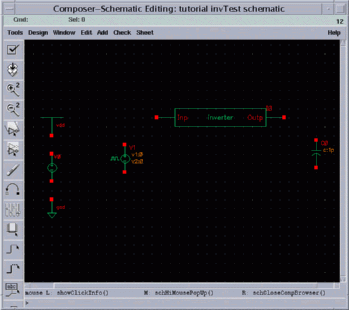
We placed all the necessary components for this schematic.
2. Why did we put these components into this schematic ?
You can think of this procedure (creating a new schematic and placing these components into the new schematic) as being analogous to building a "test-bench" for the circuit you designed. As in the real test-bench case, you must build a simple test set-up (consisting of voltage sources, load devices, etc.) around your original circuit to measure its operation and its characteristics.
a production of


Cadence is a trademark of Cadence Design Systems, Inc., 555 River Oaks Parkway, San Jose, CA 95134.
Please read this DISCLAIMER