IMPORTANT CHANGE:
These pages have a friendlier URL now :

IMPORTANT CHANGE:
These pages have a friendlier URL now :
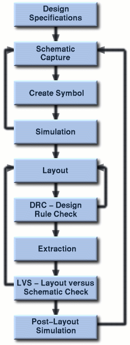
This site contains a complete on-line tutorial for a typical bottom-up design flow using CADENCE Custom IC Design Tools (version 97A). The examples were generated using the HP 0.6 um CMOS14TB process technology files, prepared at North Carolina State University (NCSU) and made available through MOSIS.
Please click on any box in the design flow (below) to see a detailed description of the corresponding design step, and to view the design examples.

a production of


Cadence is a trademark of Cadence Design Systems, Inc., 555 River Oaks Parkway,
San Jose, CA 95134.
Please read this DISCLAIMER
Last Updated by Ilhan Hatirnaz on 11/01/1998