


Note : At this point, you should have an empty schematic editor window open.
1. The first thing to do is to add and place components which will be used in the schematic.
The components we need for a schematic of an inverter are the following :
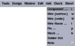
To add components, click on Add in the menu banner of the schematic
entry window and choose Component, as shown below.
( Add --> Component )
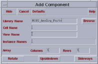
2. Two new pop-up windows appear.
One of them is "Add Component Window", where you can enter the Library Name, Cell Name and the View Name of the component to be added to the schematic.
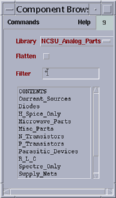
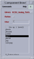
The other window is the "Component Browser", which enables the designer to browse easily through the available libraries and select the desired components.
Component Browser pops up every time the Browse button on the Add Component window is clicked.
3. We begin picking up the components by selecting the MOS transistors from the Component Browser window.
You must be careful to pick up the components from the correct library. You can change the component library simply by clicking and holding the left mouse button on the library field.
The correct library is "NCSU_Analog_Parts", so, select this library if it is not selected when you opened the Component Browser. After all, the window should appear like shown above.
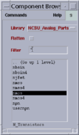
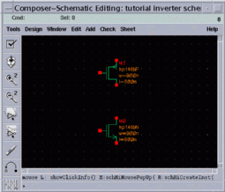
There are many folders under this library. Each of them is named depending on the components they include. So, to pick up an n-type MOSFET, you have open the "N_Transistors" folder by clicking once on it. The new folder contains many symbols which are also shown in the picture below. Pick up the NMOS transistor by clicking once on "nmos", which is a model for a three terminal n-type MOSFET.
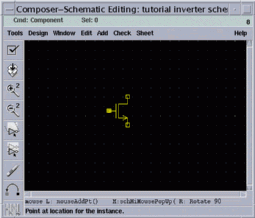
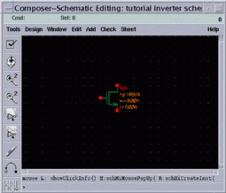
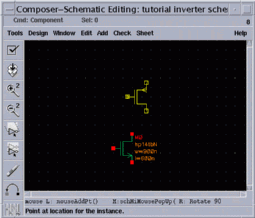
If you move the mouse cursor on the schematic window, you will see a bright NMOS transistor symbol moving with the mouse pointer showing the gate terminal of the transistor. At this point, you decide where to put this transistor. Click on a location in the schematic window, where you want to put the transistor. Please refer to the images below to see the difference between a "to be placed" transistor (left image) and "a placed transistor" (right image).
The same procedure can be applied to select and to place the PMOS transistor. The only difference is to pick "pmos" from the "P-Transistors" folder in the Component Browser. The "select-and-place" procedure for PMOS is summarized below.
Note : Always make sure that you are not confusing a PMOS transistor with an NMOS transistor. The differences between the PMOS symbol and the NMOS symbol are:
a production of


Cadence is a trademark of Cadence Design Systems, Inc., 555 River Oaks Parkway, San Jose, CA 95134.
Please read this DISCLAIMER