


1. After all the components are placed, they should be connected according to the function they realize.
To connect the components in a schematic, we use wires by choosing Add
and then Wire (narrow) on the menu banner.
( Add --> Wire (narrow) )
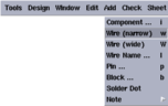
This command initiates the wiring mode.
2. A new window called Add Wire will pop-up.
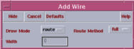
In this window you can change the routing method and the draw mode.
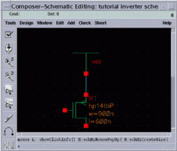
3. We begin to wire the components by connecting VDD and the source terminal of the PMOS transistor.
Every component has tiny red squares on its terminals where you can do the wiring. Connecting any two nets in the schematic is done by first clicking at one of the nets and then at the other one.
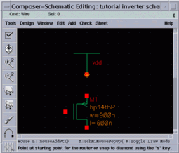
During these steps, you will always be prompted by the schematic window. The message appears in the bottom most field of the schematic window. If you follow the instructions prompted in that field, you can easily complete your job. In this step, the following phrase will be prompted :
Point at the starting point for the router
Since we begin with wiring the VDD and the source of PMOS, we click first at the center of the red square which corresponds to the VDD net.
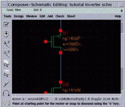
One end of the wire is now fixed, and you will realize that the other end floats and moves according to the mouse pointer. You will also see that the nearest net to the floating end of the wire is automatically highlighted. The new prompt is the following :
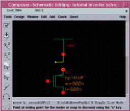
Point at ending point for the router
3. Click on the target net which is the source terminal of the PMOS transistor .
This was the final step of connecting the two nodes. The same procedure can be applied for the rest of the nodes; first choose any two nodes which should be connected. Then, wire them together just by clicking first one of them and then the other.
As long as you are in the wiring mode, you will be prompted about the next step you have to do, as described above. Press ESC on the keyboard, to leave the wiring mode. You will be in this mode, as long as you don't press ESC or choose another command from the menu.
4. The remaining steps are summarized below.
In the wiring mode,
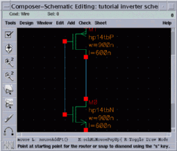
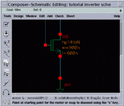
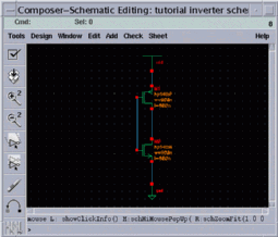
5. Your schematic should look like the schematic shown in the image below.
Press ESC key to leave the wiring mode.
a production of


Cadence is a trademark of Cadence Design Systems, Inc., 555 River Oaks Parkway, San Jose, CA 95134.
Please read this DISCLAIMER