Symbol Creation
Please follow the example link (button) for a detailed description of "Symbol Creation".

Please follow the example link (button) for a detailed description of "Symbol Creation".
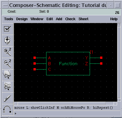
If a certain circuit design consists of smaller hierarchical components (or modules), it is usually very beneficial to identify such modules early in the design process and to assign each such module a corresponding symbol (or icon) to represent that circuit module. This step largely simplifies the schematic representation of the overall system. The "symbol" view of a circuit module is an icon that stands for the collection of all components within the module.
A symbol view of the circuit is also required for some of the subsequent simulation steps, thus, the schematic capture of the circuit topology is usually followed by the creation of a symbol to represent the entire circuit. The shape of the icon to be used for the symbol may suggest the function of the module (e.g. logic gates - AND, OR, NAND, NOR), but the default symbol icon is a simple rectangular box with input and output pins. Note that this icon can now be used as the building block of another module, and so on, allowing the circuit designer to create a system-level design consisting of multiple hierarchy levels.

a production of


Cadence is a trademark of Cadence Design Systems, Inc., 555 River Oaks Parkway, San Jose, CA 95134.
Please read this DISCLAIMER