Simulation
Please follow the example link (button) for a detailed description of "Simulation".

Please follow the example link (button) for a detailed description of "Simulation".
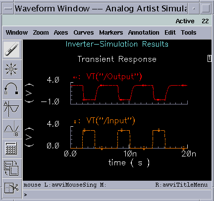
After the transistor-level description of a circuit is completed using the Schematic Editor, the electrical performance and the functionality of the circuit must be verified using a Simulation tool. The detailed transistor-level simulation of your design will be the first in-depth validation of its operation, hence, it is extremely important to complete this step before proceeding with the subsequent design optimization steps. Based on simulation results, the designer usually modifies some of the device properties (such as transistor width-to-length ratio) in order to optimize the performance.
The initial simulation phase also serves to detect some of the design errors that may have been created during the schematic entry step. It is quite common to discover errors such as a missing connection or an unintended crossing of two signals in the schematic.
The second simulation phase follows the "extraction" of a mask layout (post-layout simulation), to accurately assess the electrical performance of the completed design.

a production of


Cadence is a trademark of Cadence Design Systems, Inc., 555 River Oaks Parkway, San Jose, CA 95134.
Please read this DISCLAIMER