


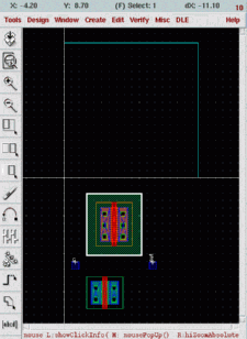
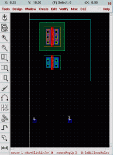
The default behavior of the layout editor is to show only the current hierarchy. You can press shift-f to display all the hierarchy levels, this way you'll be able to see actual transistors instead of the red instance rectangles.
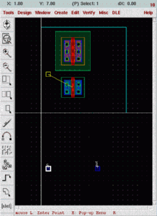
The first step is to place all the components within the design area.
1. Select the PMOS transistor by clicking once.
2. Move the selected transistor by dragging it with the mouse.
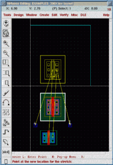
Note that in addition to the ghost image of the selected object, lines to other objects will show up. These lines represent the connections of the selected (and dragged) object to other objects of the design. In this example the poly of the PMOS transistor will be shown connected to the poly of the NMOS transistor and the input, and the drain region of the transistor will be shown connected to the output and the drain region of the NMOS.
3. Release the mouse button to place the selected transistor.
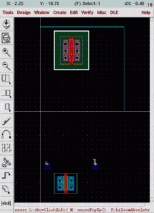
4. Move the remaining objects the same way
Note that the automatic layout tool looks almost identical to the Virtuoso layout editor. All of the commands that were available in the manual layout tool are available in this tool too. You can use rulers to pinpoint the exact location of the devices.
The I/O pins correspond to the pins drawn in the schematic. Although they just look like an ordinary Metal-1 patch they contain information about the name, type and direction of the connection.
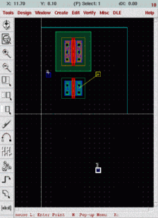
As the last step, move and place the output pin too.
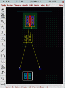
5. Final placement
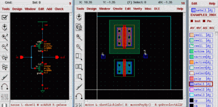
Your final working environment should look more or less like this. Note that this placement is not obligatory, you can choose to place the transistors and the I/O pins any way you desire.
a production of


Cadence is a trademark of Cadence Design Systems, Inc., 555 River Oaks Parkway, San Jose, CA 95134.
Please read this DISCLAIMER