


In the previous step we have placed the components, the next step is to make the connections between individual objects. We will be using the same methods that we used during manually drawing a layout here. The automatic layout tool has an additional menu which provides some useful options to faciliate signal connections.
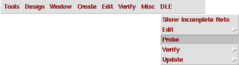
1. From the menu DLE select option Probe.
The probe option will display a small dialog box:
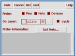
Now you can go and select connections (nets) devices, and terminals in either layout or the schematic window and the corresponding object will be highlighted in the other window. This is called cross-probing.
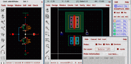
As an example try clicking and selecting the wire connecting the drains of both transistors to the output pin, notice that two drain regions as well as the output I/O pin in the layout window will be highlighted.
2. Connect the drain regions with Metal-1 using the path command.
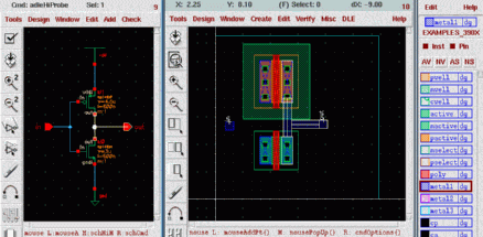
Notice that the new connection will also be highlighted as it is drawn.
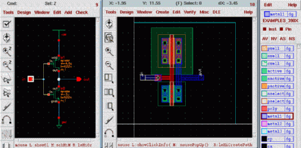
Connect the gates of both transistors using a poly path and connect this path to the input.
a production of


Cadence is a trademark of Cadence Design Systems, Inc., 555 River Oaks Parkway, San Jose, CA 95134.
Please read this DISCLAIMER