


So far you have created a number of cell views corresponding to the same circuit. In this section we want to review all of these cellviews and discuss why they are used.
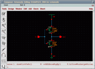
1. Schematic view
For any design, the schematic should be the first cell view to be created. The schematic will be the basic reference of your circuit.
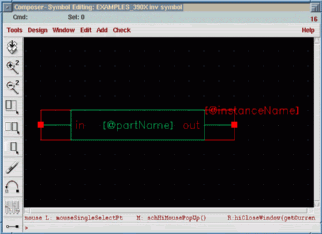
2. Symbol view
After you are done with the schematic, you will need to simulate your design. The proper way of doing this is to create a seperate test schematic and include your circuit as a block. Therefore you will need to create a symbol.
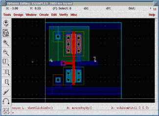
3. Layout view
This is the actual layout mask data that will be fabricated. It can be generated by automated tools or manually.
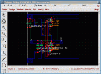
4. Extracted view
After the layout has been finalized, it is extracted, devices and parasitic elements are identified and a netlist is formed.
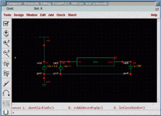
5. Test Schematic
A separate cell is used to as a test bench. This test bench includes sources, loads and the circuit to be tested. The test cell usually consists of a single schematic only.
a production of


Cadence is a trademark of Cadence Design Systems, Inc., 555 River Oaks Parkway, San Jose, CA 95134.
Please read this DISCLAIMER