


If you are not satisfied with the simulation results, there are two different aspects that can be modified :
This means that the setup to simulate your design should be modified. You can basically change two things, the properties of the input signal you feed to the circuit and the amount of output load which is capacitive. Also, make sure that the power supply voltages are connected properly.
Refer to the step "Define the voltage sources" to setup your input sources.
Refer to the step "Determine the output load" to change the capacitance value of the capacitor.
Refer to the step "Define the voltage sources" to check the connections of your power supply voltages.
These changes are made without descending to a lower level of hierarchy in the design.
Usually, you will need to change the W/L ratios (the ratio between the channel width and channel length) of the transistors to meet your design specifications. Therefore, you have to edit your design which consists only of a CMOS inverter in our example.
The procedure describing how to re-run the simulation after editing the design is summarized below.
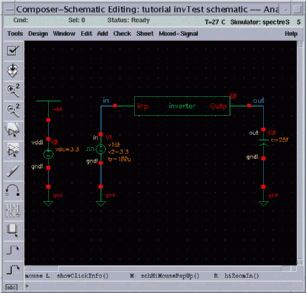
1. Go back to the schematic window and select the symbol of your design. The symbol for the inverter should be selected in this example.
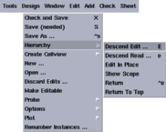
2. Click on Design in the menu banner, select Hierarchy and then Descend Edit.
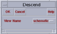
3. Click on OK in the Descend window which asks the designer which view of the design is to be edited.
The existing schematic window now displays the schematic view for the inverter, by going one level down through the design hierarchy.
4. Make the appropriate changes in the editable schematic of the design.
To change the existing W/L ratio for a specific transistor, you have to edit its object properties. Refer to the "Edit Object Properties" step in the schematic example.
5. Check and save your new schematic.
6. Click on Design in the menu banner, select Hierarchy and then Return.
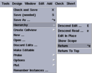
Never forget that you are editing the design at a lower level of the hierarchy - you always must return to the original level from which you have descended.
7. Go to the Analog Artist window and run the simulation again, as described in "Run the Simulation" step.
As the simulation runs, you can switch to the waveform window, because the waveforms will be updated after the simulation is finished.
You can iterate on your design as described in this section of the tutorial. When you want to end the simulation, quit the Analog Artist simulator. This will automatically close the Waveform window, too.
Note: Quitting a tool does not mean closing the corresponding window. Please always use the "close" or "quit" commands located in the menu bar of the tool.
a production of


Cadence is a trademark of Cadence Design Systems, Inc., 555 River Oaks Parkway, San Jose, CA 95134.
Please read this DISCLAIMER