


Now, we have to select the nodes that we want to observe as simulation results.
1. Click on Outputs in the menu banner, select To Be Plotted and then Select on Schematic.
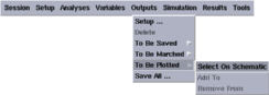
The schematic window becomes active, so that you can select the nodes to be observed in that window.
2. Click on the nets which you want to observe in the schematic window.
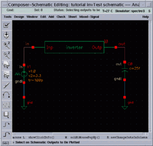
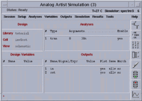
The selected nodes are the input of the inverter, "in", and the output of the inverter "out" which drives the capacitive load. Each time you select a node, the corresponding wire name appears in the Outputs list.
3. Press ESC to finish your selections.
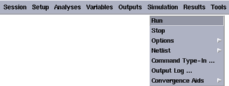
4. Start the simulation by clicking Simulation and then selecting Run.
The waveform window appears after the simulation is completed. It includes the waveforms of the selected nodes plotted between t=0 and the determined Stop Time which is 30 ns in our example.
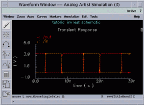
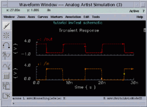
You will see the two waveforms together, plotted on the same time axis. To separate the waveforms, from the menu Axes select option To Strip. Once seperated you can select the waveforms by clicking on them and draging them on top of each other to group. To return to the initial composite waveforms, from the menu Axes select option To Composite. Notice that this option has replaced the former To Strip option.
a production of


Cadence is a trademark of Cadence Design Systems, Inc., 555 River Oaks Parkway, San Jose, CA 95134.
Please read this DISCLAIMER