


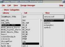
Following the extraction step a new cellview is generated in your library. This cell view is called extracted view.
Try loading the cellview. It will open up a layout that looks almost identical to the layout you have extracted. You will notice that only the I/O pins appear as solid blocks and all other shapes appear as outlines.
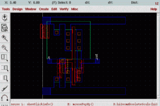
The red rectangles indicate that there are a number of instances within this hierarchy. Try pressing Shift-F to see all of the hierarchy.
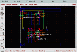
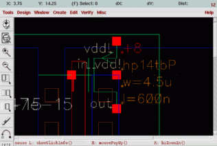
This will reveal a number of symbols. If you zoom in you will be able to identify individual elements, such as transistors and capacitors. You will notice that the parameters (e.g. channel dimensions) of these devices represent the values they were drawn in the layout view.
Apart from your actual devices you will notice a number of elements, mainly capacitors in your extracted cell view. These are not actual devices, they are parasitic capacitances, side effects formed by different layers you used for your layout.
The next step will be to correpond the extracted netlist to that of the schematic. This is called the Layout Versus Schematic checking. This will ensure that the schematic that we have drawn and the layout are identical.
a production of


Cadence is a trademark of Cadence Design Systems, Inc., 555 River Oaks Parkway, San Jose, CA 95134.
Please read this DISCLAIMER