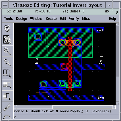

The creation of the mask layout is one of the most important steps in the full-custom (bottom-up) design flow, where the designer describes the detailed geometries and the relative positioning of each mask layer to be used in actual fabrication, using a Layout Editor. Physical layout design is very tightly linked to overall circuit performance (area, speed and power dissipation) since the physical structure determines the transconductances of the transistors, the parasitic capacitances and resistances, and obviously, the silicon area which is used to realize a certain function. On the other hand, the detailed mask layout of logic gates requires a very intensive and time-consuming design effort.
The physical (mask layout) design of CMOS logic gates is an iterative process which starts with the circuit topology and the initial sizing of the transistors. It is extremely imporant that the layout design must not violate any of the Layout Design Rules, in order to ensure a high probability of defect-free fabrication of all features described in the mask layout.

Please follow this example link for a detailed description of the main procedures in "Mask Layout Design".
Another alternative of generating the mask layout is to make use of automated tools. Please follow this example link for a detailed description of generating a layout from a schematic using the device level placer.
a production of


Cadence is a trademark of Cadence Design Systems, Inc., 555 River Oaks Parkway, San Jose, CA 95134.
Please read this DISCLAIMER